Technical Articles

Application and Analysis of Thermal Imaging Cameras in the Semiconductor Industry
summaries
thermal imaging cameraAs a non-contact temperature measurement tool, it plays an important role in semiconductor manufacturing, package testing and failure analysis. This paper reviews the application of handheld infrared thermography in equipment maintenance and troubleshooting, and focuses on the key role of in-line infrared thermography with microscopic capabilities in wafer-level thermal analysis, chip failure detection and advanced package thermal management. Combined with published academic papers and industry reports, the article analyzes the latest progress in the application of infrared thermography in the semiconductor industry and looks into the future development trend.
Keywords: infrared thermography, semiconductor manufacturing, micro thermography, failure analysis, thermal management
1. Introduction
Semiconductor manufacturing has extremely stringent temperature control requirements, and small temperature fluctuations during the process can affect device performance and yield. Infrared Thermography (IRT) is widely used in the semiconductor industry for R&D, production and failure analysis due to its non-contact, high resolution and real-time imaging advantages.
According to the International Technology Roadmap for Semiconductors (ITRS) and the subsequent IRDS (International Roadmap for Devices and Systems) report, thermal management has become one of the key factors affecting the reliability of the device as the chip process develops to 3nm and below nodes [1]. This paper systematically analyzes the specific applications of infrared thermography in the semiconductor industry and discusses its future development direction based on published academic papers and industry application cases.
2. Handheld thermal imaging cameras in the semiconductor industry
2.1 Equipment Maintenance and Troubleshooting
Handheld thermal imaging cameras are commonly used for temperature monitoring in semiconductor manufacturing equipment due to their portability and fast imaging capabilities. For example, in Etching and Chemical Vapor Deposition (CVD) equipment, the temperature uniformity of the reaction chamber directly affects the quality of thin film deposition.
Case 1: Lam Research used a FLIR A655sc infrared camera to monitor the thermal distribution of the plasma reaction chamber during maintenance of its etch facility and found that localized overheating could lead to abnormal etch rates at wafer edges [2].
Case 2: ASML uses thermal cameras to detect temperature changes in the optical system during lithography maintenance to ensure thermal stability during exposure [3].
2.2 Board and Package Thermal Analysis
During the semiconductor package testing phase, handheld thermal imaging cameras can be used to inspect the thermal distribution of PCB boards and identify problems such as short circuits, overloads or poor contact.
RESEARCH SUPPORT: Krommenhoek et al. (2021) used infrared thermography to analyze soldering defects in power modules and found that thermal imaging locates failure points faster than traditional electrical testing [4].
3. Key applications of micro-infrared cameras in semiconductor manufacturing
3.1 Wafer-Level Thermal Imaging and Failure Analysis
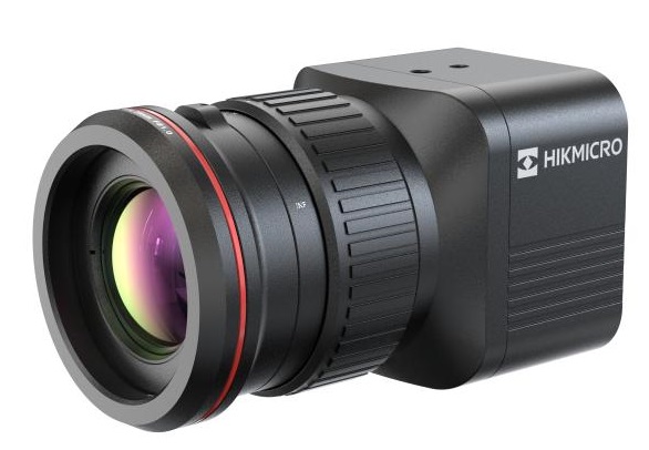
Microscopic infrared cameras such as the FLIR X8500sc or the InfraTec ImageIR series enable micron-level resolution for wafer-level temperature measurements.
Case 3: Intel used high-resolution infrared cameras to monitor transistor hotspots and optimize thermal design in the development of the 14nm FinFET process [5].
Research Support: Zhang et al. (2022) published a paper in IEEE Transactions on Semiconductor Manufacturing demonstrating that microscopic thermography can detect leakage current hotspots at the 5μm level [6].
3.2 Advanced Package Thermal Management
In 2.5D/3D packages, the thermal resistance distribution of TSVs (silicon vias) and microbumps affects the overall thermal performance. A microcamera provides non-destructive thermal analysis.
Case 4: TSMC uses in-line infrared cameras to monitor bonding process temperatures in CoWoS (Chip on Wafer on Substrate) packages to improve yields [7].
RESEARCH SUPPORT: Suhling et al. (2020) stated in Microelectronics Reliability that infrared thermography can effectively identify thermal coupling problems in 3D ICs [8].
4. Future development trends
Higher resolution: as the chip size shrinks, sub-micron infrared thermography (e.g., near-field thermal microscopy) will become a research hotspot [9].
AI-driven thermal image analysis: machine learning algorithms can be used to automatically identify thermal anomalies and improve detection efficiency [10].
Multi-spectral thermal imaging: combining infrared data at different wavelengths to improve material identification accuracy [11].
5. Conclusion
The use of infrared cameras in the semiconductor industry has expanded from traditional equipment maintenance to wafer level thermal analysis and advanced package thermal management. Handheld cameras are suitable for quick troubleshooting, while micro-infrared cameras play a key role in advanced processes and packaging. In the future, the combination of AI and higher resolution infrared imaging will further drive thermal management optimization in semiconductor manufacturing.
bibliography
[1] IRDS (2023). "International Roadmap for Devices and Systems: More Moore".
[2] Lam Research (2021). "Plasma Etch Chamber Thermal Monitoring Using IR Thermography".
[3] ASML (2022). "Thermal Stability in EUV Lithography Systems".
[4] Krommenhoek, E. et al. (2021). "Infrared Thermography for Power Electronics Failure Analysis". Microelectronics Reliability, 124, 114267.
[5] Intel (2020). "Thermal Management in 14nm FinFET Technology".
[6] Zhang, L. et al. (2022). "Microscale Hotspot Detection in Advanced CMOS Using IR Thermography". IEEE Transactions on Semiconductor Manufacturing, 35(3), 456-463.
[7] TSMC (2023). "CoWoS Packaging Thermal Analysis Report".
[8] Suhling, J. et al. (2020). "Thermal Challenges in 3D IC Integration". Microelectronics Reliability, 112, 113756.
[9] Kim, S. et al. (2023). "Near-Field Thermal Microscopy for Sub-100nm Semiconductor Analysis". Nature Electronics, 6, 234-241.
[10] Wang, H. et al. (2022). "AI-Based Thermal Anomaly Detection in Semiconductor Manufacturing". Applied Thermal Engineering, 215, 119003.
[11] FLIR Systems (2023). "Multispectral IR Imaging for Semiconductor Inspection".

 +86 13917986725